

 InfoSearched
Chipmakers ran out of light — so ASML started vaporizing tin with lasers to keep Moore’s Law alive.
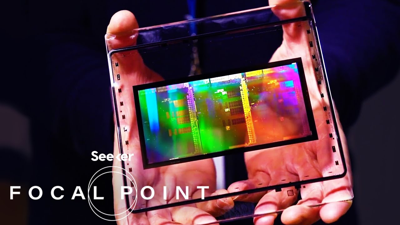
For more than a decade, the semiconductor industry treated extreme ultraviolet lithography as either the technology that would save Moore’s Law or the one that would never actually ship. By early 2020, it had shipped — and the machine behind it looks less like a factory tool and more like a physics experiment bolted to a production line.
- Extreme ultraviolet (EUV) light measures just 13.5 nanometers — a wavelength so short it borders on X-ray radiation, replacing the 193nm deep ultraviolet (DUV) light that had hit its diffraction limit.
- To generate that light, ASML’s systems fire a high-powered CO2 laser at microscopic droplets of molten tin falling through a vacuum chamber at tens of thousands of drops per second, vaporizing them into plasma.
- Developing the breakthrough took ASML more than 17 years and over €6 billion in R&D, culminating in the company’s 100th commercial EUV system shipment by early 2020.
Limitations of Conventional Optical Physics
Moore’s Law — the observation, credited to Intel co-founder Gordon Moore, that the number of transistors on a chip roughly doubles every couple of years — depends on printing features small enough to keep shrinking. Deep ultraviolet lithography, running at a 193nm wavelength, carried that job for two decades through clever workarounds like multiple patterning. But 193nm light is physically too long to resolve the nanometer-scale features modern chipmakers need, and no amount of engineering trickery could bend that limit any further.
That left the industry — Intel, Samsung, and TSMC among the buyers — needing a fundamentally shorter wavelength, not an incremental fix. EUV’s 13.5nm light gets there, but at a cost: it behaves nothing like the visible or ultraviolet light used in prior generations of lithography tools.
Turning Tin Into Plasma
EUV light doesn’t exist in any convenient natural form, so ASML’s TWINSCAN NXE:3400-series tools manufacture it on demand. Droplets of molten tin, smaller than a grain of sand, fall through the machine at a rate of tens of thousands per second. A high-powered CO2 laser strikes each droplet twice — first to flatten it into a disc, then to vaporize it into a superheated plasma that emits EUV light as a byproduct.
Because ordinary air absorbs EUV wavelengths almost instantly, that entire light-generation and printing process happens inside a high-vacuum chamber. There’s no atmosphere to interfere with the light on its path to the silicon wafer.
Mirrors Flatter Than Anything Ever Made
Glass lenses, the workhorses of every prior lithography generation, are useless here — conventional optical glass simply absorbs and refracts EUV light rather than transmitting it cleanly. ASML’s solution relies on multilayer Bragg reflective mirrors built by Carl Zeiss, engineered to some of the flattest tolerances of any manufactured surface on Earth. Light bounces off a series of these mirrors rather than passing through lenses, threading its way to the wafer without losing the precision needed to etch features measured in nanometers.
EUV uses a wavelength of just 13.5 nanometers — light so short it borders on X-ray radiation.
Sub-Nanometer Precision at Speed
None of the optics matter if the silicon wafer itself isn’t perfectly positioned. ASML’s wafer stages hold each disk in place with sub-nanometer precision, making positional corrections up to 20,000 times per second while the wafer moves beneath the beam. It’s the mechanical half of the machine doing work just as demanding as the plasma physics happening a few feet away — chip designs built for Intel’s competitive product lines and roadmaps, including systems like the Core i9 10980XE, depend on that level of repeatability holding up across millions of exposures.
Getting there wasn’t cheap or fast. ASML spent over 17 years and more than €6 billion developing EUV before it became a commercially viable production tool, and the company didn’t reach its 100th shipped system until early 2020 — a milestone that marks EUV’s shift from lab curiosity to standard equipment on the fabrication floor.
Tin plasma and Bragg mirrors aren’t the only path chipmakers are chasing to keep transistor counts climbing — some are also looking past silicon itself, toward materials like gallium oxide for the next jump in efficiency. But for now, EUV is the tool that’s actually running in production, and its 100-system count is the number the rest of the industry is watching climb.







THE FIRST EVER HOVERBIKE IN THE WORLD
Intel’s behavior is PATHETIC – Core i9 10980XE Review
This Man Launched a New Internet Service Provider from His Garage | Freethink DIY Science
What we learned from building a medical technology startup | Fouad Al-Noor | TEDxTUBerlin
Boyan Slat unveils The Ocean Cleanup Interceptor